- 您现在的位置:买卖IC网 > Sheet目录369 > W9725G6IB-25 (Winbond Electronics)IC DDR2-800 SDRAM 256MB 84-WBGA
�� �
�
�W9725G6IB�
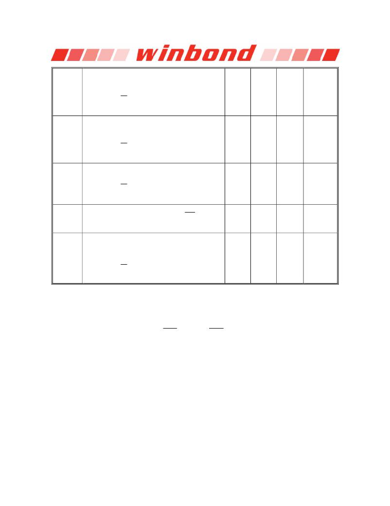
�Operating� Burst� Read� Current�
�All� banks� open,� Continuous� burst� reads,� I� OUT� =� 0� mA;�
�BL� =� 4,� CL� =� CL� (IDD),� AL� =� 0;�
�I� DD4R�
�t� CK� =� t� CK(IDD)� ;� t� RAS� =� t� RASmax(IDD)� ,� t� RP� =� t� RP(IDD)� ;�
�155�
�135�
�mA�
�1,2,3,4,5,6�
�CKE� is� HIGH,� CS� is� HIGH� between� valid� commands;�
�Address� inputs� are� SWITCHING;�
�Data� Bus� inputs� are� SWITCHING.�
�Operating� Burst� Write� Current�
�All� banks� open,� Continuous� burst� writes;�
�BL� =� 4,� CL� =� CL� (IDD),� AL� =� 0;�
�I� DD4W�
�t� CK� =� t� CK(IDD)� ;� t� RAS� =� t� RASmax(IDD)� ,� t� RP� =� t� RP(IDD)� ;�
�170�
�150�
�mA�
�1,2,3,4,5,6�
�CKE� is� HIGH,� CS� is� HIGH� between� valid� commands;�
�Address� inputs� are� SWITCHING;�
�Data� Bus� inputs� are� SWITCHING.�
�Burst� Refresh� Current�
�t� CK� =� t� CK(IDD)� ;�
�I� DD5B�
�Refresh� command� every� t� RFC(IDD)� interval;�
�CKE� is� HIGH,� CS� is� HIGH� between� valid� commands;�
�145�
�135�
�mA�
�1,2,3,4,5,6�
�Other� control� and� address� inputs� are� SWITCHING;�
�Data� bus� inputs� are� SWITCHING.�
�Self� Refresh� Current�
�I� DD6�
�CKE� ≦� 0.2� V,� external� clock� off,� CLK� and� CLK� at� 0� V;�
�Other� control� and� address� inputs� are� FLOATING;�
�4�
�4�
�mA�
�1,2,3,4,5,6�
�Data� bus� inputs� are� FLOATING.�
�Operating� Bank� Interleave� Read� Current�
�All� bank� interleaving� reads,� I� OUT� =� 0mA;�
�BL� =� 4,� CL� =� CL� (IDD),� AL� =� t� RCD(IDD)� -� 1� x� t� CK(IDD)� ;�
�I� DD7�
�t� CK� =� t� CK(IDD)� ,� t� RC� =� t� RC(IDD)� ,� t� RRD� =� t� RRD(IDD)� ,� t� RCD� =�
�t� RCD(IDD)� ;�
�195�
�170�
�mA�
�1,2,3,4,5,6�
�CKE� is� HIGH,� CS� is� HIGH� between� valid� commands;�
�Address� bus� inputs� are� STABLE� during� deselects;�
�Data� Bus� inputs� are� SWITCHING.�
�Notes:�
�1.�
�2.�
�3.�
�4.�
�V� DD� =� 1.8� V� ±� 0.1V;� V� DDQ� =� 1.8� V� ±� 0.1V.�
�I� DD� specifications� are� tested� after� the� device� is� properly� initialized.�
�Input� slew� rate� is� specified� by� AC� Parametric� Test� Condition.�
�I� DD� parameters� are� specified� with� ODT� disabled.�
�5.� Data� Bus� consists� of� DQ,� LDM,� UDM,� LDQS,� LDQS� ,� UDQS� and� UDQS� .�
�6.� Definitions� for� I� DD�
�LOW� =� V� in� ≦� V� IL� (ac)� (max)�
�HIGH� =� V� in� ≧� V� IH� (ac)� (min)�
�STABLE� =� inputs� stable� at� a� HIGH� or� LOW� level�
�FLOATING� =� inputs� at� V� REF� =� V� DDQ� /2�
�SWITCHING� =� inputs� changing� between� HIGH� and� LOW� every� other� clock� cycle� (once� per� two� clocks)� for� address� and�
�control� signals,� and� inputs� changing� between� HIGH� and� LOW� every� other� data� transfer� (once� per� clock)�
�for� DQ� signals� not� including� masks� or� strobes.�
�Publication� Release� Date:� Oct.� 23,� 2009�
�-� 41� -�
�Revision� A04�
�发布紧急采购,3分钟左右您将得到回复。
相关PDF资料
W9725G6JB25I
IC DDR2 SDRAM 256MBIT 84WBGA
W9725G6KB-25I
IC DDR2 SDRAM 256MBIT 84WBGA
W972GG6JB-3I
IC DDR2 SDRAM 2GBITS 84WBGA
W9751G6IB-25
IC DDR2-800 SDRAM 512MB 84-WBGA
W9751G6KB-25
IC DDR2 SDRAM 512MBIT 84WBGA
W9812G6JH-6I
IC SDRAM 128MBIT 54TSOPII
W9816G6IH-6I
IC SDRAM 16MBIT 50TSOPII
W9825G6JH-6I
IC SDRAM 256MBIT 54TSOPII
相关代理商/技术参数
W9725G6JB
制造商:WINBOND 制造商全称:Winbond 功能描述:4M ? 4 BANKS ? 16 BIT DDR2 SDRAM
W9725G6JB-25
制造商:Winbond Electronics Corp 功能描述:DRAM Chip DDR2 SDRAM 256M-Bit 16Mx16 1.8V 84-Pin WBGA 制造商:Winbond Electronics 功能描述:512MB DDRII
W9725G6JB25I
功能描述:IC DDR2 SDRAM 256MBIT 84WBGA RoHS:是 类别:集成电路 (IC) >> 存储器 系列:- 标准包装:150 系列:- 格式 - 存储器:EEPROMs - 串行 存储器类型:EEPROM 存储容量:4K (2 x 256 x 8) 速度:400kHz 接口:I²C,2 线串口 电源电压:2.5 V ~ 5.5 V 工作温度:-40°C ~ 85°C 封装/外壳:8-VFDFN 裸露焊盘 供应商设备封装:8-DFN(2x3) 包装:管件 产品目录页面:1445 (CN2011-ZH PDF)
W9725G6KB-18
制造商:Winbond Electronics 功能描述:IC MEMORY 制造商:Winbond Electronics Corp 功能描述:IC MEMORY
W9725G6KB-25
功能描述:IC DDR2 SDRAM 256MBIT 84WBGA RoHS:是 类别:集成电路 (IC) >> 存储器 系列:- 标准包装:1 系列:- 格式 - 存储器:闪存 存储器类型:闪存 - NAND 存储容量:4G(256M x 16) 速度:- 接口:并联 电源电压:2.7 V ~ 3.6 V 工作温度:0°C ~ 70°C 封装/外壳:48-TFSOP(0.724",18.40mm 宽) 供应商设备封装:48-TSOP I 包装:Digi-Reel® 其它名称:557-1461-6
W9725G6KB-25 TR
制造商:Winbond Electronics Corp 功能描述:256M DDR2-800, X16
W9725G6KB25A
制造商:WINBOND 制造商全称:Winbond 功能描述:DLL aligns DQ and DQS transitions with clock, Data masks (DM) for write data, Write Data Mask
W9725G6KB25I
制造商:Winbond Electronics Corp 功能描述:DRAM Chip DDR2 SDRAM 256M-Bit 16Mx16 1.8V 84-Pin WBGA 制造商:Winbond Electronics 功能描述:IC DDR2 SDRAM 256M 2.5NS 84WBGA 制造商:Winbond Electronics Corp 功能描述:IC DDR2 SDRAM 256M 2.5NS 84WBGA 制造商:Winbond 功能描述:DRAM Chip DDR2 SDRAM 256M-Bit 16Mx16 1.8V 84-Pin WBGA